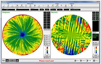
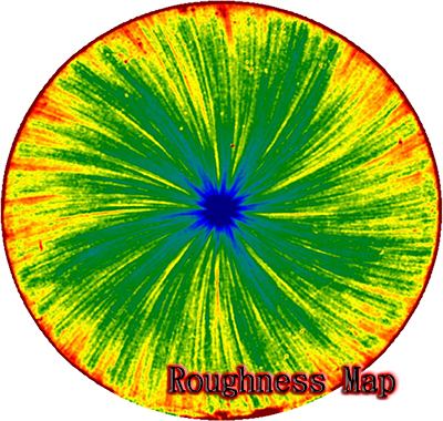
After processing SI wafer are backside ground to reduce their thickness from 700μm to < 50μm. In the last grinding step, the surface quality needs to be close to polished to keep the underlying chip structures intact.
OptoSurf has developed measurement devices based on scattered light technology that perform a fast, whole-surface scan of wafer surfaces, measuring time for a 300mm wafer is less than 30s with a resolution of Ra < 1nm